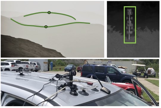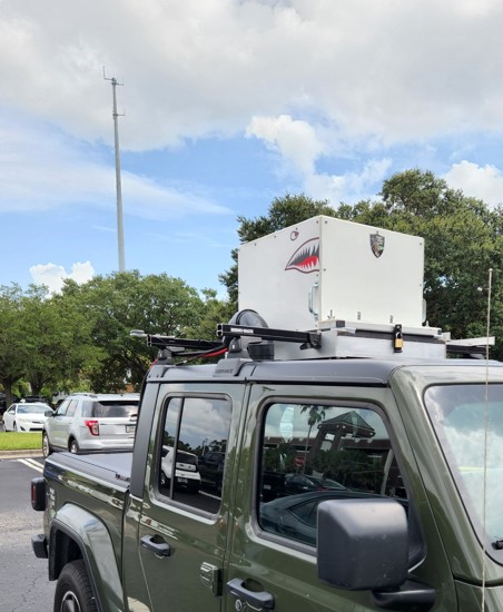
- Conducted remote sensing data collection at Eglin AFB with ARL and Chicken Little
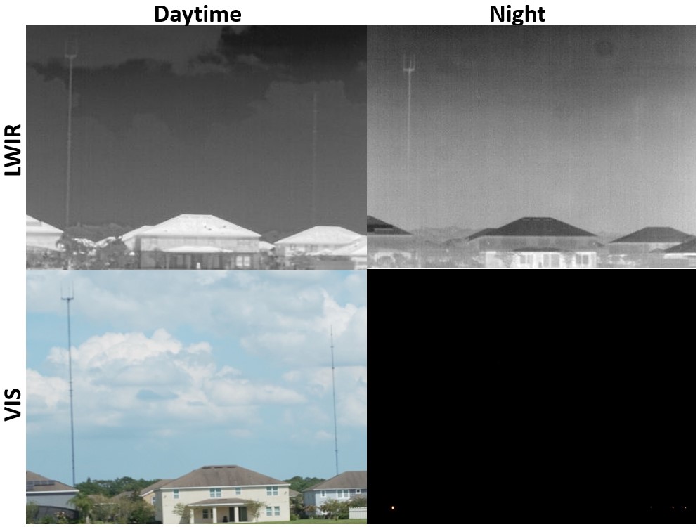
- Started round 2 for python detection – we are now building a drone-based system
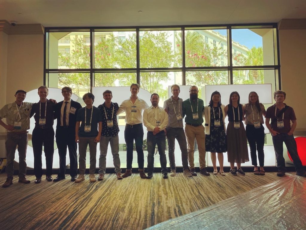
- May: KVL presents 5 papers at SPIE Defense and Commercial Sensing Symposium
- Alex graduates with his B.S. in ECE (Surprise!)
- Completed field test at Big Oaks Ranch for VISNAV and MUAS projects (see video below)
- Hank interns at Metalenz (summer)
- Li interns at Amazon, Machine Vision and Optical Engineering team (Fall)
- Congraduations to Pooya, Sajad and Zhao for defending their PhD theses this spring!
- April: 5 papers presented at SPIE Defense and Commercial Sensing – a record for KVL
- Pooya and Sajad’s paper on visible light communications came out in JLT
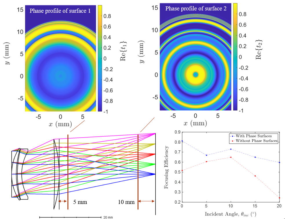
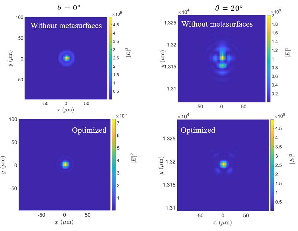
- Ko-Han’s metasurface lens paper in Opt. Exp. featured as an Editor’s Pick
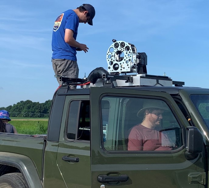
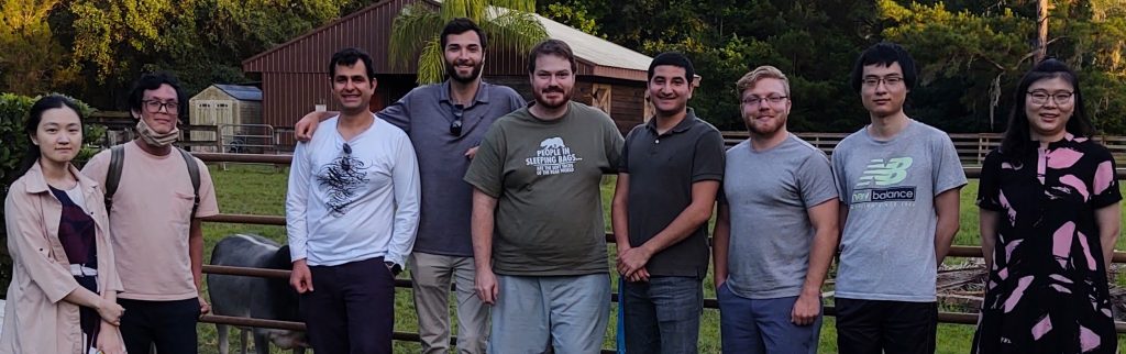
- July: 4 KVL members concluded a successful week of data collection in Memphis with collaborators
- KVL leads a $4M award to research targeting technologies for high-energy lasers
- KVL welcomes two new members, Oles and Eunmo, to do research in active targeting systems
- Congratulations to Robert for defending his PhD thesis this Fall!
- Dec: 6 KVL members participated in a data collection event in the Santa Rita Experimental Range near Tucson.
- Heath successfully defended his thesis, congratulations Dr. Gemar!
- TFO Lab changes name to Knight Vision Lab to better reflect our research focus on imaging technologies.
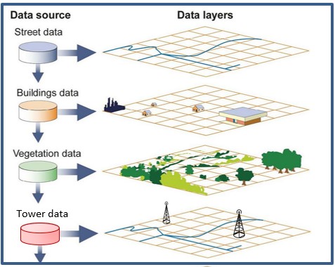
- TFO spearheads a collaboration on vision-based navigation [read more]
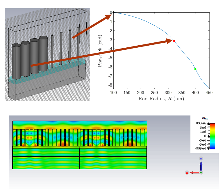
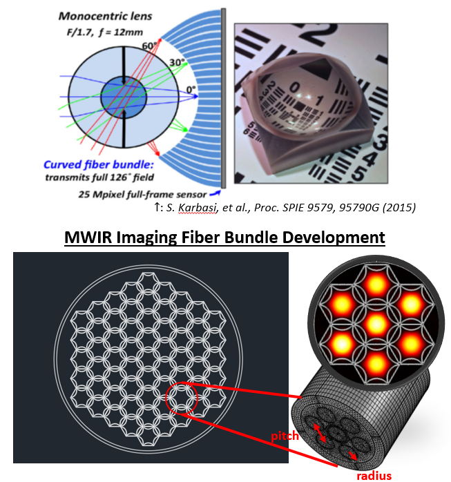
- Heath’s paper on MWIR nanoaperture filters published in Opt. Mat. Exp.
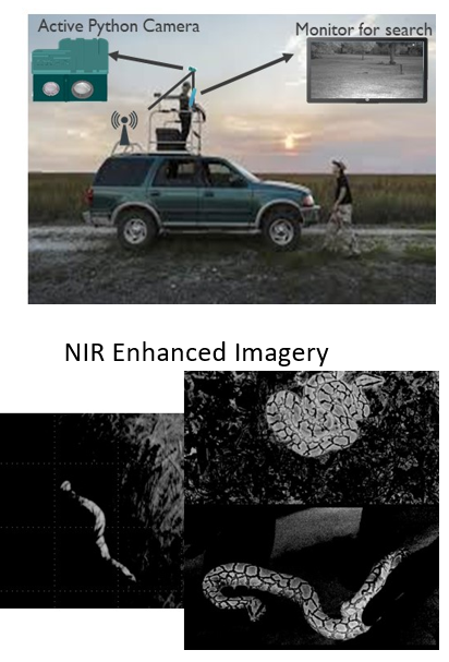
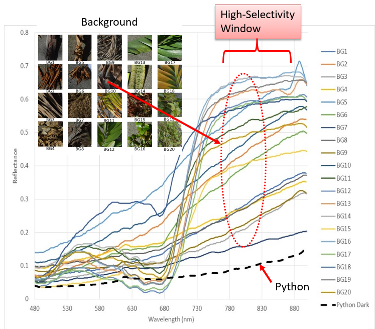
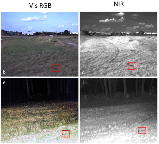
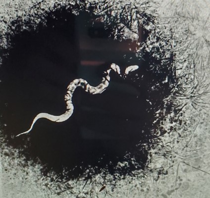
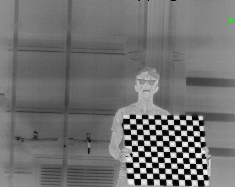
- Jen’s python detection work published in App. Opt. was featured in local [1,2] and national news [3,4]
- May 16: TFO summer party celebrates an end to COVID isolation
- Cesar wraps up his senior design and research thesis to graduate with honors!
- Robert presents thermal contrast enhancement using multiple thermal bands at SPIE DCS
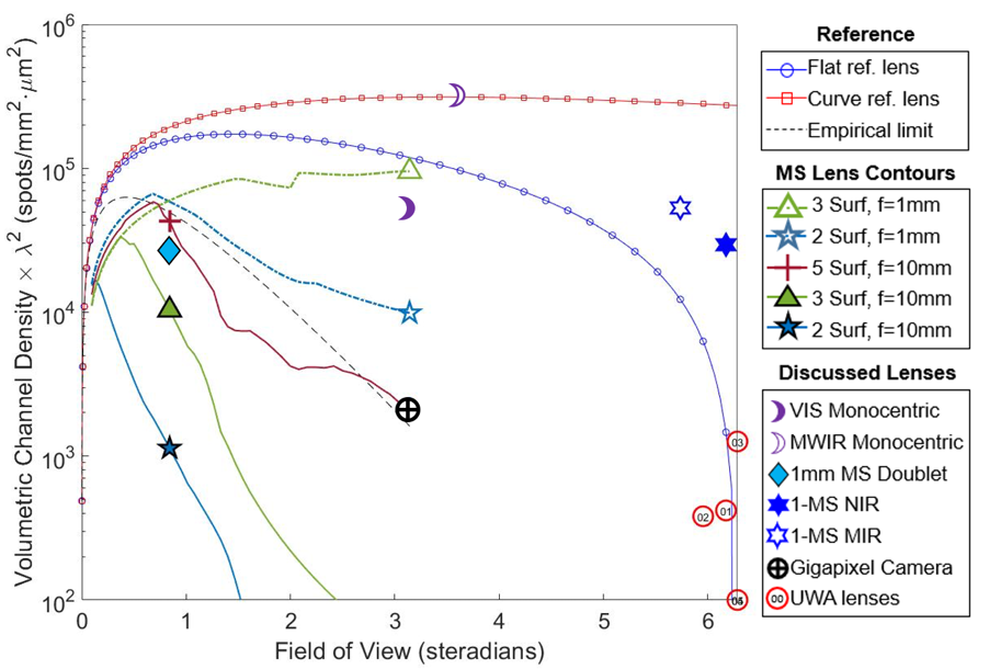
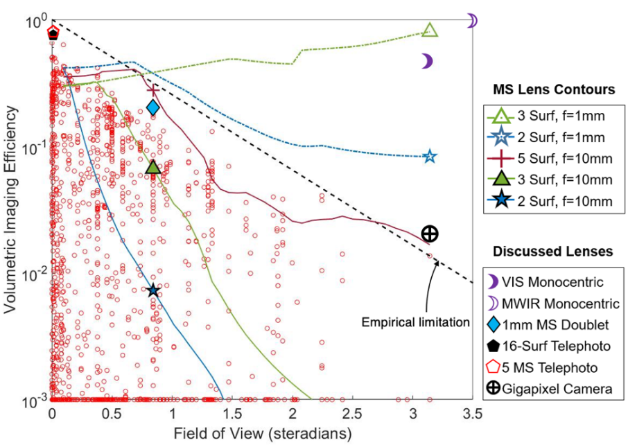
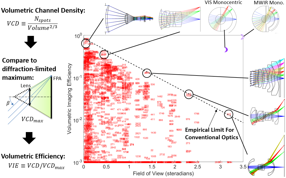
- Zhao’s Volumetric Imaging Efficiency (VIE) paper published in Opt. Exp.
- COVID happened = 2020 🙁
- Cesar wins best poster at the UofA Winter School of Optics
- Cesar wins Distinguished Undergraduate Research Award
- Sajad and Pooya present VLC Transmitter at MobiCom/LIoT
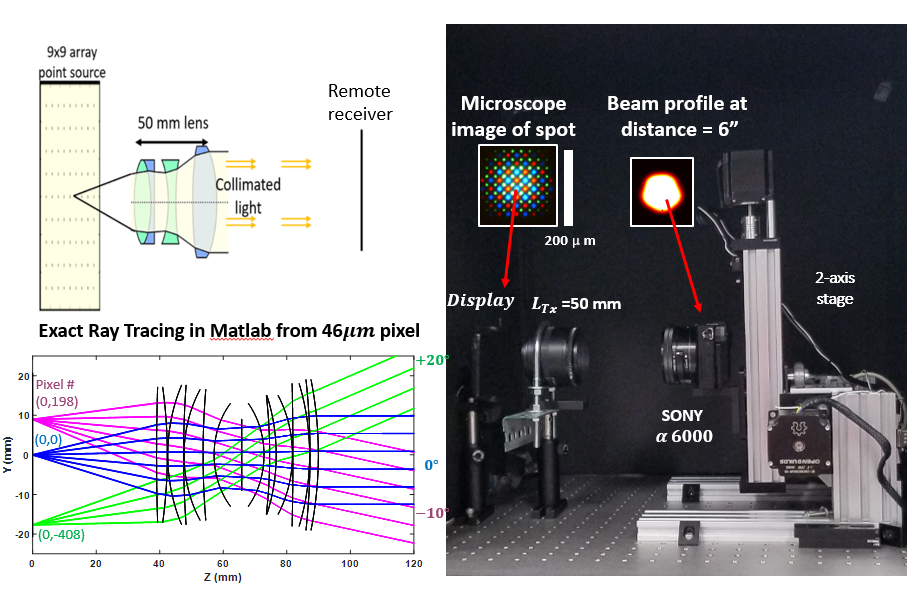
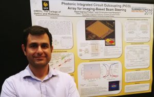
- Sajad presents PICO Array development at CLEO
- The TFO group expands: welcome new team members!
- Cesar receives Most Outstanding Summer Researcher from AFRL.
- Zhao’s JAP paper receives editor’s pick and is featured in Scilights.
- Sajad wins best poster at the IEEE Summer Topical meeting for “Photonic Integrated Circuit Outcoupling (PICO) Arrays for Free-Space Optical Communications.”
- Sajad is selected for a summer internship at IMEC-Florida.
- Sajad wins best poster at the Industrial Affiliates Symposium for “Camera/Inverse-Camera System for Free-Space Optical Communications.”
- Cesar is accepted for a summer internship at AFRL.
- Sajad presents an Inverse-Camera System for Optical Wireless Communications at Frontiers in Optics
- Dr. Renshaw presents a switchable organic photodiode at OSA Imaging Congress
- Dr. Renshaw awarded AFRL Summer Faculty Fellowship
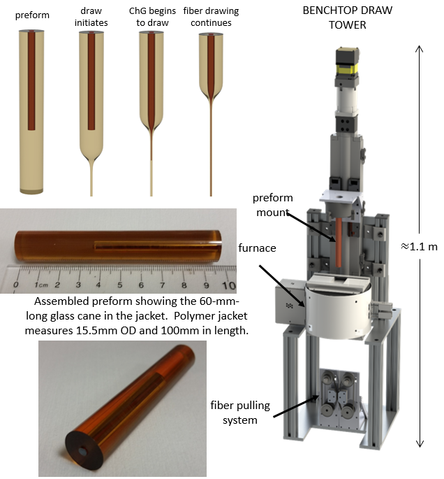
- Zhao presents a poster on curved sensor fabrication at SPIE Defense and Commercial Sensing
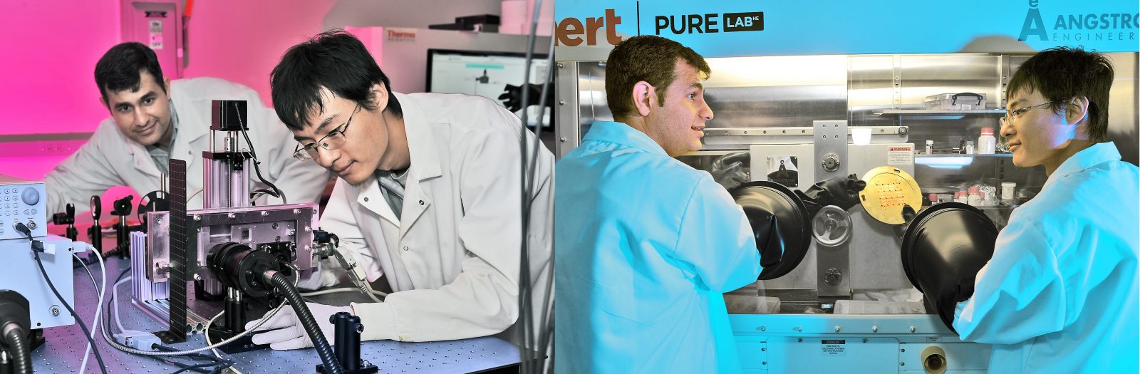
- Angstrom deposition tool is installed; first films grown and OPD/OLED devices fabricated
- TFO Lab is completed!