Imaging systems have grown to become ubiquitous pieces of technology found in an ever-increasing range of applications including cell phones, self-driving cars, and refrigerators that photograph their insides. This growth has been facilitated by mobile devices, which have driven camera technologies to smaller form factors and lower cost. Despite individual component advances and the transition to digital sensors, the basic design of camera systems have not changed over the past century; a complex lens is designed to flatten the object scene onto a flat image sensor – but this is about to change.
There are enormous optical advantages to replace the conventional flat sensor with a curved image sensor due to field curvature effects, which cause optical systems to naturally focus to curved surfaces. For example, biological imagers such as the human eye utilize a curved sensor (i.e. the retina) matched to the curved focal surface of a simple lens. This approach provides superior imaging performance in a simple, compact system. Availability of curved image sensors will decouple the traditional constraints between field-of-view (FOV), resolution and image quality; this will enable the biggest revolution in camera systems since the development of digital image sensors. Recent advances in flexible electronics are paving the way to enable the fabrication of curved image sensors and consumer camera manufacturers have already begun erecting intellectual property fences to capitalize on this innovation.
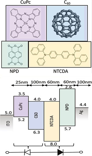
The Thin-Film Optoelectronics (TFO) group at CREOL, directed by Kyle Renshaw, is pioneering fabrication technologies to enable the manufacture of curved image sensors for visible and infrared cameras. The group is pursuing two independent solutions to this challenging problem. The first solution is based on a novel class of materials, organic molecular semiconductors, which can be fabricated directly onto curved glass or plastic substrates. Devices can be fabricated on the curved surface using a high-resolution stamp- transfer patterning processes. This process enables patterning submicron features across the curved surface using a lithographically defined stamp. The team has demonstrated organic photodiodes sensitive across the visible spectrum and into the near infrared with quantum efficiency > 25% and dynamic range > 105.

With the devices and processing technology in place, the team is now developing the technology to scale these photodiodes into mid-sized arrays (<1 megapixel) suitable for ultracompact, wide-FOV imagers. The approach utilizes a novel pixel architecture that leverages layer-by-layer growth capabilities with a simple two-terminal design to minimize the patterning complexity on the curved surface. This vertically-stacked anti-polar diode (VAD) pixel architecture combines an organic photodiode with a blocking diode in a single vertically integrated stack. The result is a pixel with nearly 100% fill factor that only requires two patterning steps with lenient registration requirements. This pixel can be readily fabricated on the curved surface and provides read-out control suitable to address mid-sized arrays. This solution will provide ultracompact, low-cost, wide FOV imagers ideally suited for vision-based navigation systems.

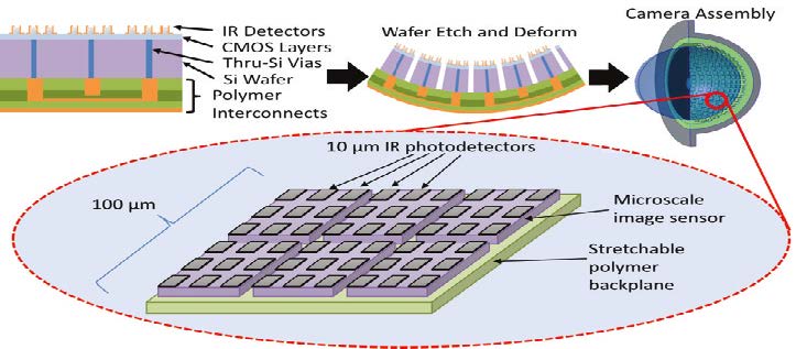
The TFO group is also developing a second solution to realize curved image sensors based on silicon CMOS read-out integrated circuits (ROICs) – a fundamentally planar technology. This approach will enable large arrays suitable for high-resolution visible or infrared imaging by leveraging mature CMOS technology and hybridization processes that allow integration of infrared sensitive photodetectors on ROICs. The group is developing a stretchable polymer backplane that is monolithically integrated on the backside of a novel ROIC wafer. This ROIC contains a mosaic of microscale image sensors interconnected through the stretchable backplane. An anisotropic etch between each microscale sensor is used to segment the ROIC wafer and transform the original, rigid, wafer- based circuit into a stretchable circuit carried by the polymer backplane. The stretchable circuit can be deformed into the desired shape using a mold; the group has demonstrated deformation of single-layer interconnects on polymer substrates up to 120° of a hemisphere.
Author
