
We design the photons and the electrons to work together — then grow, fabricate and characterize the materials and devices that prove they do.
Epitaxial Nanophotonics & Integrated Design
The design philosophy underneath everything else in the lab.
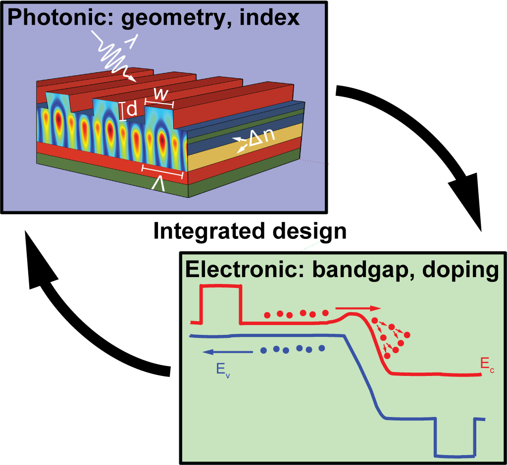
Optoelectronic device design usually privileges the electron over the photon. The APD Lab’s core belief is that epitaxial nanophotonics, coupled with an integrated design approach, is pivotal to advancing next-generation optoelectronic devices.
That means working in two paradigms at once. In the photonic paradigm we manipulate material geometry and permittivity to strengthen light–matter interaction. In the electronic paradigm we tune band structure to amplify functionality or serve the photonic design. Holding both together demands a comprehensive understanding of the electronic, photonic, and atomic attributes of semiconductor materials.
The payoff has been a broad family of enhanced devices across many materials, wavelengths, and applications — brighter luminescence, improved device response, lower noise, and substantially higher detector operating temperatures.
Quantum-limit Devices
Nanophotonic avalanche photodiodes chasing single-photon sensitivity.
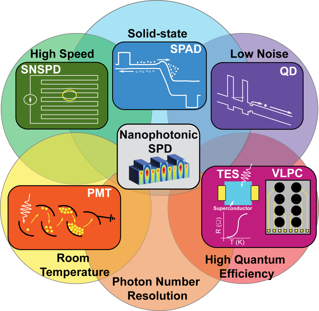
Epitaxial nanophotonic avalanche photodiodes (APDs) hold significant promise for quantum-limit single-photon detectors (SPDs). No single SPD technology today possesses every necessary characteristic at once, and that gap is the opening we work in. Our emphasis is on the design, growth, fabrication, and thorough characterization of nanophotonic SPDs.
The reach extends well past quantum information science. APDs underpin medical imaging — fluorescence lifetime imaging microscopy, positron emission tomography, Cherenkov detection — as well as LIDAR and other consumer sensing.

UVC Laser Diodes
Pseudomorphic digital alloys for a laser diode that has resisted the field for decades.
A practical, electrically injected laser diode in the ultraviolet-C remains one of the outstanding challenges in compound semiconductor optoelectronics. We approach it through pseudomorphic digital alloys — short-period AlN/GaN superlattices grown strain-matched to the underlying template — which decouple the composition needed for deep-UV gain from the dislocation generation that ordinarily accompanies it.
This work runs on Pomelo, the lab’s nitride MBE system, with its nitrogen plasma source, scandium cell, and custom photo-enhanced growth capability.
High-index Nanophotonics
Exotic modes that only exist once the refractive index is high enough.
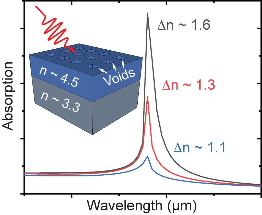
Some optical modes are simply unavailable at low index contrast. We identify and explore nanophotonic structures supporting modes exclusive to high-index systems — guided mode resonances, bound states in the continuum, and Mie-type photonic modes — then put them to work in real detectors and emitters.
Hybridizing these resonances is how we push infrared detector performance and operating temperature past what a conventional absorber-limited design allows.
Projects and funding
5 active awards support the work above.
Pseudomorphic Digital Alloys for Resilient UVC Laser Diodes
PIDigital-alloy AlGaN heterostructures grown pseudomorphically to push ultraviolet-C laser diodes toward practical, radiation-resilient operation. Supports the group's nitride MBE effort on “Pomelo.”
Part of UVC Laser Diodes
Nanophotonic Mid-wave Infrared Avalanche Photodiodes
PIPairing epitaxial nanophotonic resonances with avalanche gain to approach quantum-limit single-photon detection in the mid-wave infrared. Selected from a pool of more than 150 proposals.
Part of Quantum-limit Devices
High-index Hybrid-mode Nanophotonic Infrared Detectors
PIExploiting hybridized guided-mode and Mie-type resonances available only in high-refractive-index systems to raise infrared detector performance and operating temperature.
Part of High-index Nanophotonics
High Power Adaptive Wavefront Control
Co-PIMaterials and device work supporting adaptive wavefront control at high optical power.
Electrically Switchable Reflective Amplitude Modulator in the MWIR
PIA reflective, electrically switchable amplitude modulator for the mid-wave infrared, built on the group's epitaxial nanophotonics platform.
Completed awards & user programs
Including Center for Integrated Nanotechnologies (CINT) user proposals, which provide facility access rather than direct funding.
Exploring the Ultimate Limits of Non-degenerate two-photon absorption
PIPart of Quantum-limit Devices
Pulsed Laser-Assisted Synthesis of Materials for American-made semiconductors (PLASMAs)
Co-PIHeteroepitaxial light emitting diodes for infrared scene projection applications
PIEpitaxial Heterojunction Lead-Selenide Photovoltaic Detectors for High-density Focal Plane Arrays
PIRoadside Fog Detection Sensor Aging Studies of Camera Sensing Material Platform
Co-PINanophotonic short-wave infrared single-photon avalanche photodiodes
PIAdvancing Light-Matter Interaction through High-Index Nanophotonics in the Mid-Infrared Range
PIAdvancing Light-Matter Interaction through High-Index Nanophotonics in the Mid-Infrared Range
PIAcknowledgment
Any opinions, findings, and conclusions or recommendations expressed on this site are those of the authors and do not necessarily reflect the views of the Army Research Office, the Air Force Office of Scientific Research, the Department of Defense, Sandia National Laboratories, or the University of Central Florida.