The NPM Group is developing new processes for creating functional passive and active photonic materials and devices. Our approach involves using multi-photon 3D microfabrication (3DM) coupled with other conventional fabrication techniques to pattern materials and devices into tailored micro- and nano-scale structure. We are using 3DM to create waveguides, optical couplers, and photonic crystals that can be directly incorporated with active photonic elements.
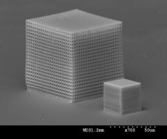
Scanning electron microscopy image of a polymeric photonic crystal created by the NPM Group using 3DM
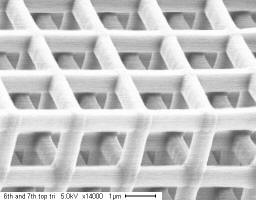
Close-up view of a polymeric photonic crystal.
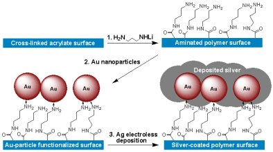
We are also exploring how surface functionalization chemistry can be coupled with 3DM as a means for creating tailored photonic materials with controlled micro- and nano-scale structure. We have developed a process for conformally depositing silver and other noble metals onto the surface of polymeric 3D micron-scale structures prepared by 3DM. The method enables us to create conductive structures and micro- and nano-photonic materials with unusual optical properties. More information on the process we have developed can be found in the publication listed below.
“Fabrication and characterization of three-dimensional silver-coated polymeric microstructures” Yun-Sheng Chen, Amir Tal, David B. Torrance, and Stephen M. Kuebler Adv. Funct. Mater., 2006, vol. 16(13), pp. 1739-1744.
Process used to deposit silver conformally onto the surface of a polymeric microstructure.
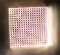
Reflection microscopy image of a conducting silvered polymeric lattice.